Voltage in → voltage out · unit V/V.
Electronics Engineering · CHAPTER 02 · FOCUSED LESSON
Operational Amplifiers
Differential gain, feedback, essential circuits, signal conditioning and real-world limits.
FROM ALI’S ORIGINAL ENGINEERING NOTESCOMPLETE, EXTENDED & VERIFIED
01 · WHY AMPLIFICATION EXISTS
The signal is already speaking. The op-amp makes it usable.
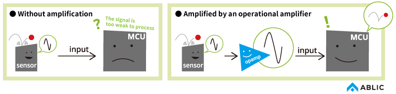
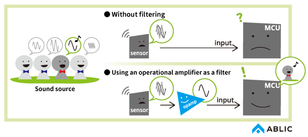
The transistor story leads to two different worlds: digital systems mainly use transistors as switches, while analogue and optical systems still need weak information-bearing signals to be strengthened, filtered and conditioned.
An operational amplifier—an op-amp—is an integrated differential voltage amplifier. It compares two input voltages and drives one output. External feedback then turns its enormous raw gain into a precise, repeatable mathematical function.
DIGITALtransistor as a switch→ANALOGUEop-amp as a signal processor
02 · SYMBOL, TERMINALS & OPEN-LOOP MODEL
It amplifies a difference—not either input alone.
The non-inverting input is marked +, the inverting input −, and the output polarity follows the sign of V+ − V−. Power-supply pins limit how far the output can move.
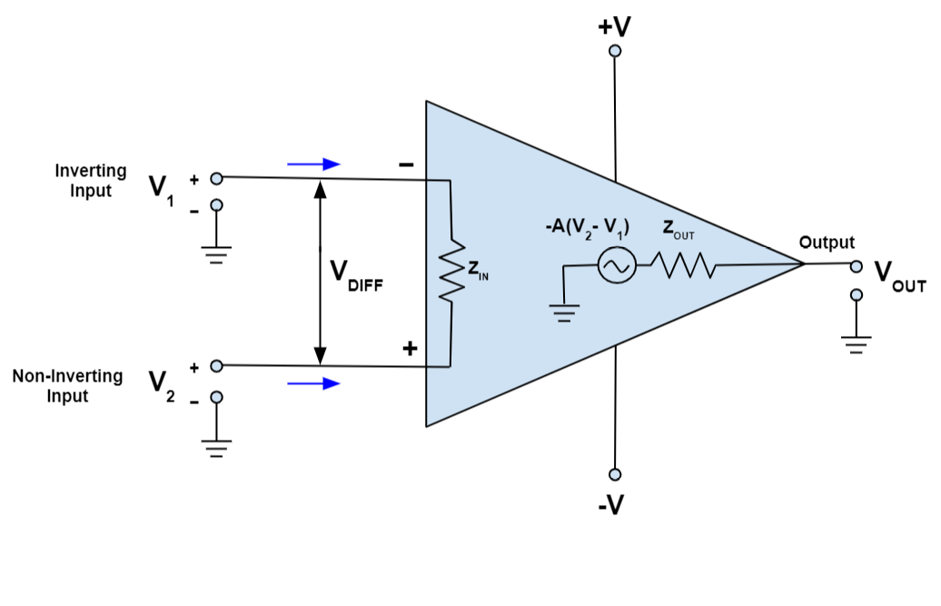
OPEN-LOOP EQUATIONVout=AOL(V+ − V−)
V+ Non-inverting input voltage · volt (V)
V− Inverting input voltage · volt (V)
AOL Open-loop differential voltage gain · V/V, dimensionless
Vout Output voltage · volt (V), limited by the supplies and output stage
Source correction: the original illustration writes −A(V₂−V₁). With V₂ labeled non-inverting and V₁ inverting, the physically consistent relation is A(V₂−V₁).
Current in → current out · unit A/A.
Voltage in → current out · siemens (S).
Current in → voltage out · ohm (Ω).
The source calls these four ways to classify op-amps. More precisely, an ordinary op-amp is fundamentally a differential voltage amplifier; suitable feedback networks let the complete circuit realize all four transfer types.
03 · WHAT THE CIRCUIT DOES FOR A REAL SIGNAL
Amplify what matters. Reject what does not.
An op-amp is rarely used alone. Resistors, capacitors and feedback define the operation: gain, filtering, summation, subtraction, buffering or comparison.
01Audio amplifiers02Low-dropout regulators03Active filters04Medical sensor interfaces05Baseband receivers06Analog-to-digital converters07Oscillators08Signal generators09Hearing aids
04 · IDEAL OP-AMP RULES
Two golden rules—with one essential condition.
The familiar rules apply to an ideal op-amp operating with negative feedback, inside its input common-mode range, output swing, bandwidth and slew-rate limits.
Ideal input impedance is infinite, so neither input draws current. Real devices have small input-bias currents.
Negative feedback drives the differential voltage extremely close to zero. The inputs are not physically shorted, and this rule fails in saturation or open-loop operation.
An ideal voltage output has zero impedance. A real op-amp has finite output resistance and strict current limits.
Real open-loop gain is merely very large and frequency-dependent. Without feedback, microvolts of differential input can drive the output into a rail.
Important distinction: “V+ ≈ V−” is the virtual-short consequence of negative feedback in linear operation. It is not the definition of zero input-offset voltage.
05 · FEEDBACK CONTROLS THE AMPLIFIER
Trade raw gain for precision and usable bandwidth.
Open loop is extremely sensitive and usually saturates. Negative feedback returns an opposing fraction of the output, forcing a stable closed-loop relationship set mainly by external components.
Huge but uncontrolled
Vout=AOL(V+ − V−)Useful as a comparator concept, but not as a precise linear amplifier.
Controlled linear gain
V−←βVoutReduces closed-loop gain but improves precision, linearity and bandwidth.
Regeneration
V+←βVoutReinforces change; useful for hysteresis and oscillators, not ordinary linear amplification.
Voltage follower
Vout≈VinUnity voltage gain with high input and low output impedance: an excellent buffer.
06 · THE TWO BASIC AMPLIFIER CIRCUITS
One inverts. One preserves polarity.
Both derivations use the same ideal rules: input current is zero and the two input voltages are nearly equal under negative feedback.
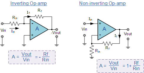
Output is 180° inverted
1 · V+ IS GROUNDED, SO V− ≈ 0V−≈V+=0
2 · NO CURRENT ENTERS THE OP-AMPVinRin=−VoutRf
3 · CLOSED-LOOP GAINVoutVin=−RfRin
Output keeps the input polarity
1 · VIN DRIVES V+V−≈V+=Vin
2 · THE DIVIDER RETURNS PART OF VOUTVin=VoutRgRf + Rg
3 · CLOSED-LOOP GAINVoutVin=1+RfRg
Replacing Rf with a potentiometer makes the gain adjustable, but the permitted resistance range must still respect stability, input-bias-current, noise and output-swing requirements.
07 · INTERACTIVE SIGNAL LAB
The equations stop being abstract here.
Change the resistor ratio, signal amplitude, frequency and supply. The same graph reveals phase inversion, closed-loop gain, finite bandwidth and rail clipping.
INTERACTIVE CLOSED-LOOP LAB
Linear closed-loop operationSee gain, inversion, bandwidth and clipping together
Signal gain-10.00 V/V
Noise gain11.00
Estimated bandwidth90.9 kHz
Actual output peak5.00 V
Av=−RfRinfCL≈GBPANEducational model: GBP = 1 MHz, dominant-pole response, and output swing ≈ 1 V inside each supply rail. Real limits come from the chosen datasheet.
08 · GAIN–BANDWIDTH PRODUCT
More closed-loop gain usually means less bandwidth.
For a dominant-pole, voltage-feedback op-amp, the closed-loop noise gain and bandwidth are approximately linked by a nearly constant gain-bandwidth product.
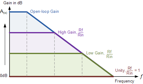
fCL: closed-loop −3 dB bandwidth in hertz. GBP: gain-bandwidth product in hertz. AN: noise gain in V/V, dimensionless.
Voltage ratios are often plotted in decibels. A gain of 10 V/V is 20 dB; 100 V/V is 40 dB.
Source correction: open-loop gain AOL is not the same thing as GBP. A high GBP does not automatically make an op-amp unstable; stability depends on phase margin, the feedback network, loading and layout.
09 · DIFFERENTIAL & SUMMING AMPLIFIERS
Subtract one signal. Add many signals.
These circuits turn Kirchhoff’s laws into analogue mathematics. Precision depends on accurate resistor ratios, not just nominal resistor values.
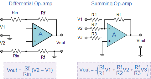
The output is proportional to the difference between two input voltages. Matched ratios reject voltage common to both inputs.
Each input receives its own weight. Equal input resistors produce the negative of the ordinary sum.
Input buffers plus a precision differential stage measure tiny sensor differences riding on a large common voltage.
10 · REAL-WORLD LIMITS
An ideal equation is the beginning of design.
Before choosing a part, compare the circuit’s needs with the datasheet across supply voltage, temperature, load and frequency.
A small internal differential voltage creates output error even when the external inputs should be equal.
Real inputs draw current; source resistance converts it into an additional voltage error.
Both input voltages must remain inside the permitted range relative to the supply rails.
The output cannot exceed its rails or source unlimited current; rail-to-rail performance is load-dependent.
Feedback remains stable only while loop gain and phase leave sufficient margin.
Large, fast signals are limited by maximum dV/dt even when the small-signal bandwidth seems sufficient.
Voltage noise, current noise and resistor thermal noise can bury microvolt-level information.
Clipping destroys waveform information and recovery can take time; feedback cannot correct beyond the output limit.
MASTER IDEAThe op-amp supplies raw gain.
The op-amp supplies raw gain.
Feedback defines the operation.
Identify the feedback path, verify that negative feedback is active, apply I+ = I− = 0 and V+ ≈ V−, derive the closed-loop equation, then check supply rails, input range, load, bandwidth, slew rate, stability and noise.