Electronics Engineering · CHAPTER 02 · FOCUSED LESSON

Transistors

Switching, amplification and the device that powers modern electronics.

FROM ALI’S ORIGINAL ENGINEERING NOTESCOMPLETE, EXTENDED & VERIFIED

The component that made electronics disappear inside everything.

Before the transistor, electronic machines depended on vacuum tubes: large, hot, fragile devices that consumed substantial power. Then, in 1947 at Bell Laboratories, John Bardeen and Walter Brattain demonstrated the point-contact transistor; William Shockley soon developed the junction-transistor concept. Their work opened a radically different era.

By about 1960, solid-state transistors were rapidly replacing tubes because they could be far smaller, cheaper, cooler and more reliable. The decisive consequence was scale: once a switch could be microscopic, engineers could place millions—and later billions—inside one integrated circuit.

1900sVacuum-tube control1947First working transistor1950sSilicon devicesTodayBillions per chip
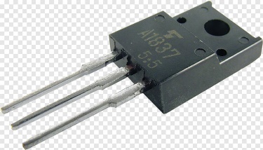
Three-terminal power transistor package from Ali Chourba's engineering notes
ORIGINAL DOCUMENT FIGUREA transistor is physically small, but its three terminals can control significant current and power.

A small electrical signal controls a larger one.

The transistor does not manufacture energy. A small signal at its control terminal regulates energy delivered by a separate power supply to a load.

01 · AMPLIFIER

Preserve the message. Increase its strength.

A microphone may produce a tiny changing signal. Biased in its forward-active region, the transistor uses that small variation to control a larger collector-current variation, producing a stronger copy for a speaker or later circuit stage.

small inputlarger output
02 · SWITCH

Represent OFF and ON.

In cutoff, collector current is nearly zero: logic 0 or switch OFF. In saturation, the transistor conducts strongly with a small collector–emitter voltage: logic 1 or switch ON. Digital chips and memories build computation from enormous networks of these states.

0CUTOFF1SATURATION
BEYOND THE TWO BASICS

Control, shape and generate signals.

The same principle supports current sources, oscillators, regulators, radio-frequency stages, sensor interfaces, motor drivers and logic gates. “Amplifier” and “switch” are the two mental models from which the rest grows.

Purity first. Then controlled imperfection.

Early transistors used germanium. Late-1950s purification and manufacturing advances made silicon practical; silicon is abundant, economical and generally tolerates higher junction temperatures than germanium.

Extremely pure crystal

Semiconductor behavior is sensitive to minute contamination. The source notes emphasize purity on the scale of roughly one unwanted atom per billion in early material processing.

Intentional doping

Adding selected donor atoms such as phosphorus, arsenic or antimony supplies mobile electrons and creates n-type silicon. Acceptor doping creates p-type material with holes as majority carriers.

Historical temperature advantage

Ali’s notes contrast roughly 200 °C silicon operation with germanium degradation above about 85 °C. Treat these as historical illustrative values: the safe maximum is always device-specific and comes from its datasheet.
Three layers. Two junctions. Three terminals.

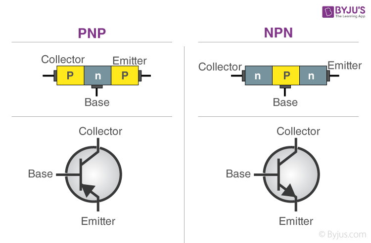
A BJT is “bipolar” because both electrons and holes participate. Two same-polarity semiconductor regions surround the opposite type, producing NPN or PNP construction.

PNP and NPN layer structures and circuit symbols from Ali Chourba's notes
ORIGINAL DOCUMENT FIGUREPNP and NPN layers with their symbols. The emitter arrow identifies the type: NPN points out; PNP points in.
B

Base

The extremely thin control region. The name comes from early construction, where it formed the physical base on which the other regions were built.

E

Emitter

Heavily doped to inject—or “emit”—majority charge carriers into the base.

C

Collector

Collects most carriers that cross the base and is usually designed to handle more voltage and dissipate more heat.

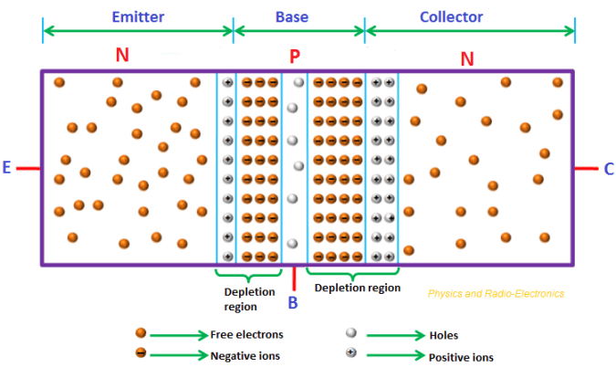
NPN emitter base collector carrier movement and depletion regions from Ali Chourba's notes
ORIGINAL DOCUMENT CARRIER VIEWThe base–emitter junction is forward biased; the base–collector junction is reverse biased during forward-active operation.
1

Injection: electrons leave the NPN emitter and enter the very thin, lightly doped base.

2

Small recombination: a minority recombines in the base, producing the base current IB.

3

Collection: most electrons reach the reverse-biased collector junction and are swept into the collector, creating IC.

4

PNP mirror: polarities and conventional-current directions reverse; holes are the majority carriers.

The relationships behind the three terminals.

Current continuity is exact. The gain ratios are operating-point parameters—not universal constants—and must be checked in the datasheet.

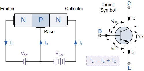
NPN transistor currents IE IB IC and voltages VBE VCB VCE from Ali Chourba's notes
ORIGINAL DOCUMENT RELATION DIAGRAMEvery current and voltage named in the equations is located on the same NPN structure and symbol.
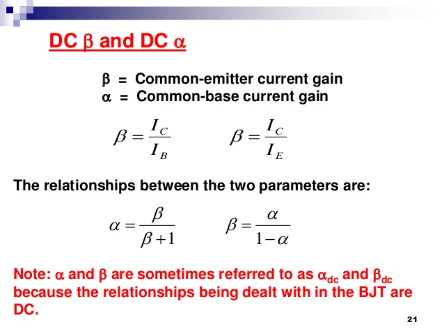
Original DC alpha and beta relationship sheet from Ali Chourba's notes
ORIGINAL DOCUMENT GAIN SHEETThe source illustration is retained. Its second gain label is corrected below: α = IC/IE, not β = IC/IE.
KIRCHHOFF CURRENT LAWIE=IB+IC

IE, IB and IC are emitter, base and collector currents, measured in amperes (A).

COMMON-EMITTER DC GAINβDC=ICIB

β is dimensionless. Ali’s notes quote roughly 20 for some power devices to more than 1000 for selected low-power devices, with about 50–200 common—but it varies strongly with current, temperature and part.

COMMON-BASE DC GAINαDC=ICIE

α is dimensionless and slightly below 1. Ali’s notes give a typical low-power range of 0.950–0.999.

CONVERT BETWEEN GAINSα=ββ + 1andβ=α1 − α

Both identities follow directly from IE = IB + IC.

TERMINAL VOLTAGEVCE=VCB+VBE

VCE is collector-to-emitter voltage, VCB collector-to-base and VBE base-to-emitter, all measured in volts (V).

SILICON BASE–EMITTER JUNCTIONVBE0.6–0.7 V

This is a useful first approximation, not a fixed law. VBE changes with collector current, temperature and the specific transistor.

“Common” names the shared terminal.

The input and output each use two terminals. The terminal shared by both sides gives the configuration its name.

COMMON EMITTER

Gain + inversion

High voltage, current and power gain. Output voltage falls when the input rises, so the voltage signal is inverted. The most common starting point for amplification and switching.

COMMON COLLECTOR

Buffer

Also called an emitter follower. Voltage gain is approximately 1, but current gain is useful. High input and low output impedance make it excellent for isolation and impedance matching.

COMMON BASE

High frequency

Current gain α is below 1, but voltage gain can be substantial. Low input impedance and good high-frequency behavior suit radio-frequency and specialized stages.

A small base variation becomes a larger, inverted voltage.

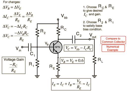
Ali’s source diagram uses a voltage-divider bias and an emitter resistor. The derivation below rebuilds every step at readable size and states the approximation being used.

Common-emitter voltage-divider amplifier and derivation from Ali Chourba's notes
ORIGINAL DOCUMENT AMPLIFIERThe complete source schematic and handwritten calculation are preserved without cropping.
1 · INPUT REACHES THE BASEΔVB=ΔVin
2 · VBE IS NEARLY CONSTANT FOR SMALL SIGNALSΔVEΔVB
3 · EMITTER CURRENT CHANGESΔIE=ΔVEREΔIC
4 · COLLECTOR VOLTAGE MOVES OPPOSITEΔVout=−ΔICRC
APPROXIMATE UNBYPASSED VOLTAGE GAINAv=ΔVoutΔVinRCRE
BASE–EMITTER BIASVBVE+0.6–0.7 V
EMITTER CURRENTIE=VEREIC
COLLECTOR BIASVC=VCCICRC
1 · SET THE SIGNAL GAIN|Av|RCRE

Choose the RC/RE ratio from the desired small-signal gain, then verify that the chosen quiescent current and supply leave enough undistorted voltage swing.

2 · SET THE BASE VOLTAGEVBVE+0.6–0.7 V

The emitter voltage fixes IE through RE; the base divider must then establish a voltage about one junction drop higher.

3 · CHOOSE THE DIVIDER RATIORRVBVCCVB

This unloaded-divider relation rebuilds the R₂/R₁ step in the source notes. In a practical circuit, base current loads the divider, so its current is made comfortably larger than IB and the final bias is recalculated.

The gain −RC/RE assumes an unbypassed emitter resistor, a sufficiently stiff bias network, small-signal operation and a load much larger than RC. Real design must include the transistor’s small-signal emitter resistance and the external load.

The circuit—not β alone—sets the final current.

Move the controls. Watch the active relation IC ≈ βIB stop being valid when the collector load reaches its physical current ceiling.

INTERACTIVE OPERATING-REGION LAB

One transistor, two jobs

Forward-active · amplifier
VCC = 9 VLoadRC = 1000 ΩCEBControlIB = 55 µAsmall IBlarger ICTHE TRANSISTOR DOES NOT CREATE POWERIB controls energy supplied by VCC to the load.
Collector current5.50 mA
Collector–emitter voltage3.50 V
Active-model request5.50 mA
Load-current ceiling8.80 mA
ACTIVE MODELICβIB

Valid only in the forward-active region.

LOAD LIMITIC,max=VCCVCE(sat)RC

Once this ceiling is reached, more base drive cannot create the βIB current predicted by the active model.

Teaching model: VCE(sat) = 0.2 V. Real β and VCE(sat) depend on the transistor, current, temperature and circuit; switching designs normally use deliberate overdrive and verify the datasheet limits.

CUTOFFBoth junctions not driven forward

IB ≈ 0 and IC ≈ 0. The transistor behaves like an open switch.

FORWARD-ACTIVEBE forward · BC reverse

IC ≈ βIB. This is the useful linear amplifier region.

SATURATIONBoth junctions forward biased

VCE is low, typically around 0.1–0.3 V. The external circuit limits IC; the transistor is ON.

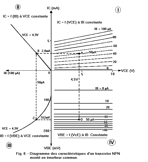
Four graphs. One transistor. One operating point.

The original diagram connects output, transfer, input and feedback characteristics. Read A → B → C → D as synchronized projections—not as four unrelated experiments.

Four-quadrant common-emitter NPN transistor characteristics from Ali Chourba's engineering notes
ORIGINAL DOCUMENT QUADRANT GRAPHThe complete figure is displayed with object-fit contain, preserving every axis, curve, dashed construction line and A–D point.
I · TOP RIGHT

Output characteristic

IC = f(VCE) for a fixed IB. Each curve is a different base current. The low-voltage knee is saturation; flatter curves are forward-active operation.

II · TOP LEFT

Transfer characteristic

IC = f(IB) for fixed VCE. Its local slope expresses current gain. In the source point, 50 µA produces 2.8 mA.

III · BOTTOM LEFT

Input characteristic

IB = f(VBE) for fixed VCE. Because the base–emitter junction is a diode, this relation is exponential rather than perfectly linear.

IV · BOTTOM RIGHT

Feedback characteristic

VBE = f(VCE) for fixed IB. It shows the smaller dependence of input voltage on output voltage at a chosen base current.

SOURCE OPERATING POINT

IB = 50 µA · IC = 2.8 mA · VCE = 4.5 V

β=2.8 mA50 µA=56Convert units first: 2.8 mA = 2800 µA.

α=5656 + 10.9825About 98.25% of emitter current reaches the collector.

IE=2.8 mA+0.05 mA=2.85 mAEmitter current equals collector plus base current.

Scientific reading note: the source graph labels VBE ≈ 162 mV at point C. That is not a typical forward-biased silicon BJT value at ordinary currents; a practical first estimate is about 0.6–0.7 V. The interactive model below therefore keeps the source graph intact but uses a physically plausible silicon VBE.

SYNCHRONIZED FOUR-QUADRANT MODEL

Move one operating point through all four views

IC = 2.80 mA · VBE = 0.651 V
ABCDI · OUTPUT · IC = f(VCE) at constant IBII · TRANSFER · IC = f(IB) at constant VCEIII · INPUT · IB = f(VBE) at constant VCEIV · FEEDBACK · VBE = f(VCE) at constant IBVCE (V)IB (µA)IC (mA)VBE (V)

The interactive curves are a smooth educational silicon model, not a replacement for a manufacturer’s datasheet. Their job is to show that A, B, C and D are four coordinated views of the same bias point.

IMPORTANT CORRECTION TO THE SOURCE NOTES

Electrons move faster than holes in silicon.

The document correctly notes that NPN devices became especially common, but its carrier-mobility explanation is reversed. In silicon, electron mobility is higher than hole mobility; this generally gives NPN transistors faster transport and better performance for comparable geometry. The notes also state that PNP production once required about three times more wafer area. That figure is process-specific rather than a universal device law: historical manufacturing and negative-ground circuit conventions did favor NPN, while modern complementary processes deliberately use both NPN and PNP devices.

MASTER IDEA

The base does not power the load.
It controls the path from the supply.

Start every BJT problem by identifying the configuration, terminal currents, junction biases and operating region. Then decide whether IC ≈ βIB is valid—or whether cutoff, saturation, the load line or a datasheet limit controls the answer.